
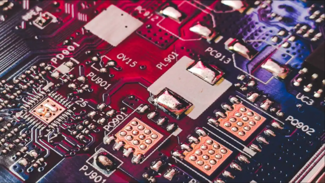
New AI apps like ChatGPT have proliferated recently. Denser and more powerful computer chips are needed for natural language chatbots. Bulk materials—3D structures—are used to make semiconductor chips. Thus, stacking transistors for denser integrations is difficult.
According to an MIT press release, researchers have developed a new method to “grow” layers of 2D transition metal dichalcogenide (TMD) materials on top of a fully fabricated silicon chip to enable denser integrations.
Growing 2D materials directly on a silicon device demands temperatures of roughly 600 degrees Celsius, which could damage silicon transistors and circuits. According to the press statement, MIT researchers have invented a low-temperature procedure to grow them without damaging the chip and directly incorporate 2D semiconductor transistors. Nature Nanotechnology published it.
2D materials increase integrated circuit density. We’re building high-rises.
In the news release, Jiadi Zhu, an electrical engineering and computer science graduate student and co-lead author of a paper on this new technique, said, “Thanks to heterogeneous integration, we have silicon as the first floor and then we can have many floors of 2D materials directly integrated on top.”
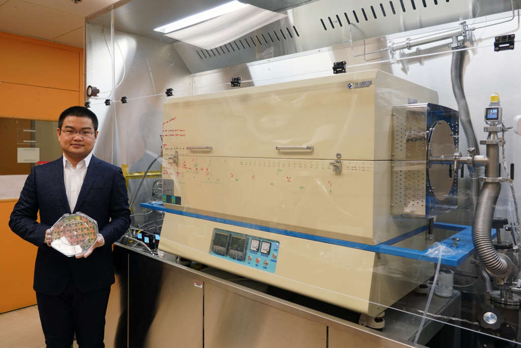
New technology can also speed up 2D material growth. It can cover 8-inch wafers in TMD material in under an hour. This allowed researchers combine a 2D material layer into bigger surfaces. The news statement says these benefits make this revolutionary approach suitable for commercial use.
The researchers want to improve this technology to apply low-temperature growth on polymers, fabrics, and papers. This could integrate electronics into clothing and notebooks.